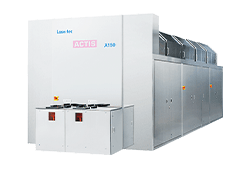
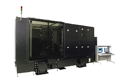
SiC Wafer Inspection and Review System
SICA88
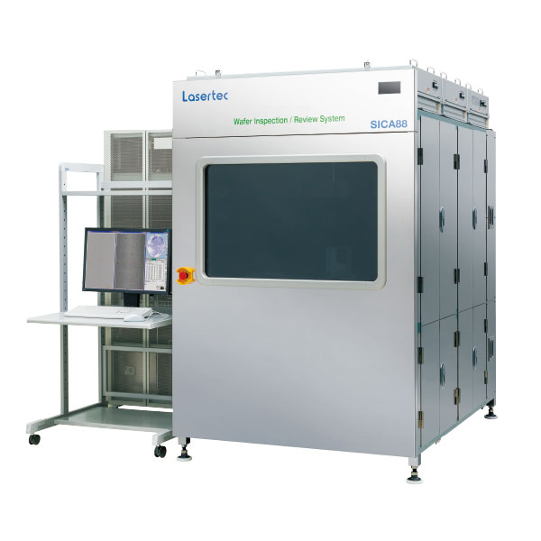
Featuring both surface and photoluminescence (PL) inspection capabilities in one body
Topics
Features
- Concurrent inspection of various surface defects and Epi layer BPD/SF
- High accuracy Automatic Defect Classification (ADC) by virtue of ultra-high resolution review images
- High throughput (10 WPH with 6 inch wafer)
Applications
- Incoming and outgoing inspection of bare SiC wafers and SiC Epi wafers
- Monitoring of SiC polishing and epitaxial growth processes
- Management of SiC device manufacturing processes