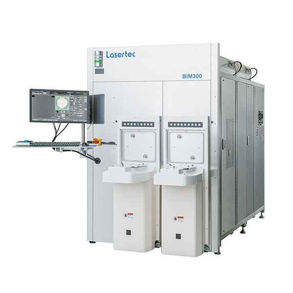
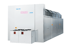
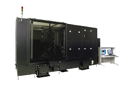
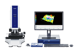
Fully Automated Wafer Measurement System
BIM Series

For highly accurate 3D profile measurement of samples that come in various sizes
Features
- Performing accurate measurement of height, width, and depth using confocal optics
- Enabling surface profile measurement not only for Si wafer samples but also for transparent samples, including SiC wafers and other compound semiconductor materials, and glass panels
- Offering different wavelengths of light including visible light and NIR, enabling the profile measurement of shapes on the surface of wafers as well as those under silicon layers
Applications
- 3D measurement of Si wafers and compound semiconductor materials, including SiC wafers, and capture of high-resolution review images
- Measurement of the height and width of redistribution layers (RDLs) on glass substrates in panel-level packaging processes
- Profile measurement of sub-surface patterns and defects inside Si wafers
Specifications
| Sample sizes | 2 inch – 12 inch (300mm) wafers, 500mm – 600mm large panels |
|---|---|
| Other | Fully automated processing compatible with SECS/GEM |


