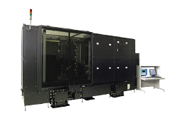
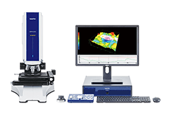
Wafer Inspection and Review System
MAGICS Series M5640

High sensitivity defect inspection/review system, implementing minute defect detection required by the next generation processes
Topics
*"MAGICS" is an abbreviation of Multiple image Acquisition for Giga-bit pattern Inspection with Confocal System.
Features
- High-sensitivity inspection of killer defects such as PID, shallow scratch, COP, and SF.
- High-throughput inspection thanks to 63 scanning laser beams and a specially designed high-speed XY stage.
- High-sensitivity inspection of mirror-polished wafers, epitaxial wafers, SOI wafers, quartz wafers and other film-coated wafers.
- High-speed high-resolution review of defect images based on confocal optics.
- Dust-free marking by diamond indenter for easy navigation and analysis using different tools such as SEM and AFM.
- Wafer handling selectable between the following 2 alternative methods:
- For outgoing and incoming inspection of wafers: Edge grip, non-back-contact chuck.
- For evaluation and analysis of wafers: Vacuum chuck applicable to wafers of multiple sizes (6, 8, and 12 inches) - Handling of FOUP, FOSB and open cassettes
Applications
- Evaluation and improvement of wafer manufacturing process
- Outgoing and incoming inspection of wafers
- Development of polishing and cleaning materials
Specifications
| Wavelength of inspection light source used for inspection | 532nm |
|---|---|
| Maximum inspection sensitivity | 50 nm (for inspection of PSLs on mirror-polished wafers) |
| Inspection time | 22 minutes per wafer (for 300 mm-wafers, normal scan) |
| Review time | 2 seconds per defect |

